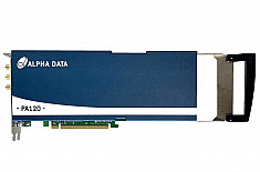
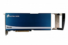
Specification
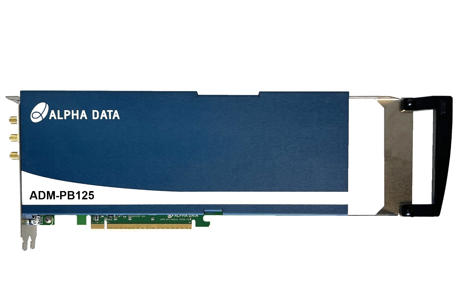
Board Format
PCIe 3/4 Length, full height, Dual Slot, includes front panel
Width: 267.2 mm
Height: 126.3 mm
Depth: 39.9 mm
Environmental Specifications
Temperature Limits | Operating Temperature Range | Storage Temperature Range |
|---|
| Min | Max | Min | Max |
|---|
| Active | FAN Fitted | 0°C | +55°C | -40°C | +85°C |
| Passive | FAN not Fitted | 0°C | +55°C | -40°C | +85°C |
Operating Humidity Range:
Up to 95% (non-condensing)
EMC:
See the ADM-PB125 Declaration of Conformity document
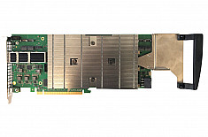
Host I/F
PCI Express Gen4x16 or 2x Gen5x8
Target Device
AMD Versal™ Premium Adaptive SoC
VP2502 (B3340)
FPGA Resources
| Chosen Device | LUTs | DSPs | BRAM | URAM |
|---|
| VP2502 | 1.71M | 7.39K | 89Mb | 366Mb |
FPGA Hard IP Cores
2x ARM Cortex-A72 MPCore™
2x ARM Cortex-R5F MPCore™
1x 256kB On-Chip Memory with ECC
472x AI Engines Tiles
On Board Memory
| Memory Type | No. Banks | Memory Size (per bank) |
|---|
| LPDDR4-SDRAM | 4 | 1G x 64 bit (8 GiB per bank) LPDDR4-3900 |
System Monitor
The ADM-PA120 provides a system monitoring chip which can provide real-time temperature, voltage and current readings of the system, as well as reconfigure programmable clocks and much more. The system monitor can be accessed directly through the USB interface via the front panel (or rear of the board). It also connects to the target FPGA via the USB to UART interface (see block diagram).
Target FPGA Configuration
The FPGA is configurable using a front panel USB interface and the Vivado tool suite (through the onboard Digilent module).The configuration flash for the FPGA is writeable via the USB interface and the Vivado tool suite, or the provided Alpha Data firmware.
FPGA Configuration Flash
| Flash Type | Flash Size |
|---|
| 8-bit QSPI | 4Gb (2x 2 Gb devices) |
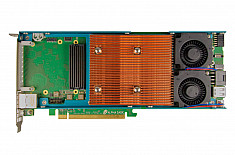
I/O Interfaces
| Interface Type | Qty | Description |
|---|
| FRONT I/O (Front Panel) |
| QSFP-DD | 1 | 3x QSFP-DD Cages for copper or fibre interconnectivity. Capable of up to 28 Gbps NRZ (all QSFP-DD cages) or 56 Gbps PAM4 (2 of the QSFP-DD cages). |
| TIMING I/O I/O (Front Panel) |
| 10-MHz external input clock | 1 | 10-MHz input (Signaling as per ITU-T G.703 section 20) |
| 1PPS Input | 1 | 1PPS timing input (Signaling as per ITU-T G.703 section 19.2) |
| 1PPS Output/Trigger Output | 1 | 1PPS timing output (Signaling as per ITU-T G.703 section 19.2) |
| Time Of Day (ToD) | 1 | RJ45 Connector for ToD and 1PPS input/Output (Signaling as per ITU-T G.703 section 19.1) |


