FFSS-ADA-VA330

Summary

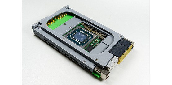
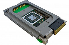
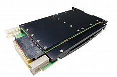
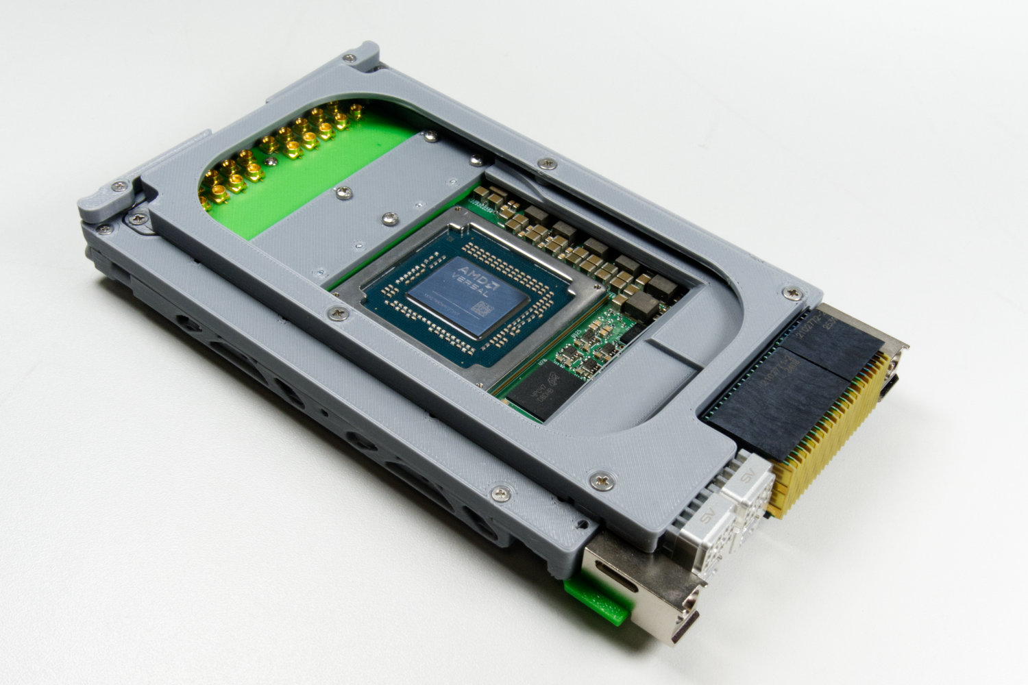
An FPGA Full System Stack (FFSS) for 14.6.11 SOSA-Aligned 3U VPX Versal RF module with PS or PL-based NVMe data streaming.

This FFSS combines the MLE NVMe PS or PL Subsystem with Alpha Data's ADA-VA330 Board featuring the AMD Versal(TM) RF VR1602 for 16 DACs and 16 ADCs at 14-bit resolution with up to 18GHz bandwidth combined with powerful hardened IP for FFT, channelization, LDPC decode, and resample. All key functionality is pre-integrated and pre-validated and ships as a compilable FPGA design project along with an IP-Core license from MLE. The FFSS-ADA-VA330 comprehensively manages the data path, configuring the PCIe core for high-speed transfer. Implementations using either the PS and PL are available depending on the customer use case.

Applications

RF Signal Sampling/Generation
Electromagnetic Spectrum Operations (EMSO)
Radar/Sensor Recording
MilCom
RF Signal Sampling/Generation
Beamforming
Signal Detection/Jamming
Pre-6G Systems

Board Features

14-bit x 16 ADC and 16 DAC channels capable of Multi-Gigasample data conversion
AMD Versal hardened and re-configurable logic and DSP processing
AMD Versal multi-core control and computation Processing System
18GHz front end bandwidth

FPGA Features (Hard IP)

16x 14-bit 8GSPS RF-ADC
16x 14-bit 16GSPS RF-DAC
2x ARM® Cortex™-A72 (APU)
2x ARM® Cortex™-R5F (RPU)
2x 100G Multirate Ethernet MAC
1x PCIe Gen5x4 (or Gen4x8)
4x DDR5 Memory Controllers

Specification

Board Format

3U VPX (SOSA Aligned - VITA 46 and 65)
Width: 160 mm
Height: 100 mm
Depth: 12.72 mm
Weight: TBD g

Environmental Specifications

Temperature Limits
Operating Temperature RangeStorage Temperature Range
MinMaxMinMax
CC1Conduction Cooled Industrial-40°C+85°C-55°C+100°C

Operating Humidity Range:
Up to 95% (non-condensing)


Host I/F

PCI Express Gen5x4(or Gen4x8)
2x Ethernet (100G/4x25G/4x10G/1x10G)


Target Device

AMD Versal RF
VR1602 (VSVA2488)

FPGA Resources

Chosen DeviceDSPsBRAMURAM
VR1602225639Mb100Mb

FPGA Hard IP Cores

16x 14-bit 8GSPS RF-ADC
16x 14-bit 16GSPS RF-DAC
2x ARM® Cortex™-A72 (APU)
2x ARM® Cortex™-R5F (RPU)
2x 100G Multirate Ethernet MAC
1x PCIe Gen5x4 (or Gen4x8)
4x DDR5 Memory Controllers

On Board Memory

Memory TypeNo. BanksMemory Size (per bank)
SDRAM432Gb LPDDR5 - 32-bit
microSD116GB 50MHz

Target FPGA Configuration

PS - Configured via OSPI or uSD


FPGA Configuration Flash

Flash TypeFlash Size
OSPI2Gb

On-board Clock Specifications

250MHz Reference Clock- HSSIO MGTs
Programmable Clock (156.25MHz default)
300MHz Reference Clock (LPDDR5)
300MHz Fabric Clock
25MHz Reference Clock (Ethernet)
33.33MHz Reference Clock (PS Core)
External Analog Reference Clock


I/O Interfaces

Interface TypeQtyDescription
ANALOG I/O (VPX Aperture)
High-Frequency Analogue Inputs1614-bit 8GSPS RF-ADC BW 18GHz
Connector: SMPS (Aperture H)
High-Frequency Analogue Outputs1614-bit 16GSPS RF-DAC BW 18GHz
Connector: SMPS (Aperture H)
DISCRETE I/O (VPX Aperture)
Digital I/O8Reference Clocks and Synchronization
Connector: SMPS (Aperture H)
DISCRETE I/O (P1)
General Purpose I/O1GPIO (single ended)
PROCESSOR I/O I/O (P1)
Low-Speed Serial I/O2Maintenance Port (2)
HIGH-SPEED DIGITAL I/O (P1)
High-Speed Serial I/O1Control Plane - 10G Ethernet
High-Speed Serial I/O1Data Plane - 10/25/40/100G Ethernet
High-Speed Serial I/O1Data Plane - 10G Ethernet
High-Speed Serial I/O1Expansion Plane - x4 PCIe Gen 5
P0 COMMUNICATIONS I/O (P0)
Serial Low-Speed Comms2IPMC compliant redundant I2C
ONBOARD COMMS I/O (Front I/O)
Onboard USB Comms 1JTAG and System Monitor
Connector: USB-C connector
Onboard USB Comms 1FPGA USB Interface
Connector: USB-C connector
uSD Configuration Interface1uSD Configuration Interface
Connector: uSD connector
DISCRETE I/O (Front I/O)
General Purpose I/O34 GPIO (Differential or Single Ended)
Connector: D-Sub GPIO Connector

Ordering Information

Ordering Code
FFSS-ADA-VA330(i)(d)(s)(r)(c)(a)
ParameterCodeParameter Description
Stack IPi-NVMePL-x4 = PLx4,
-NVMePL-x1 = PLx1
-NVMePS = PSx4
Deviced/1602 = XCVR1602
/1652 = XCVR1652
Speed Grades-2MSE = -2MSE
RF Front I/Or/WB = Wideband high-density from I/O
/PASS = Pass-through passive I/O
Coolingc/CC1 = conduction cooled industrial
Conformal Coatingablank = no conformal coating
/A = Acrylic
/P = Polyurethane
NotePlease Contact sales for other options.

Related Products

ADA-VA330

ADA-VA330

RF Signal Sampling/Generation

A Versal RF VR1602/VR1652 Adaptive SoC based 14.6.11 SOSA-Aligned 3U VPX module. This module delivers all the advantages of AMD's latest RF platform, in a common industry standard and deployable form factor.

View Product

FFSS-ADA-V9202

FFSS-ADA-V9202

RF Signal Sampling/Generation

An FPGA Full System Stack (FFSS) 3U VPX RFSoC module integrated with PL-based NVMe data streaming.

View Product

Resources:

Reference Designs: (FFSS-ADA-VA330-PLx)

Download Reference Designs []


Deliverables

FFSS-ADA-VA330 Board
One-Year Warranty
One-Year Technical Support

Support

Please contact Alpha Data for full details on the available support packages for the FFSS-ADA-VA330.

Sales Questions

Sales Questions

For any sales questions please e-mail us at [email protected]

Sales Questions

Technical Support

For any technical questions please e-mail us at [email protected]

Get in touch and request a quote


Contact Us